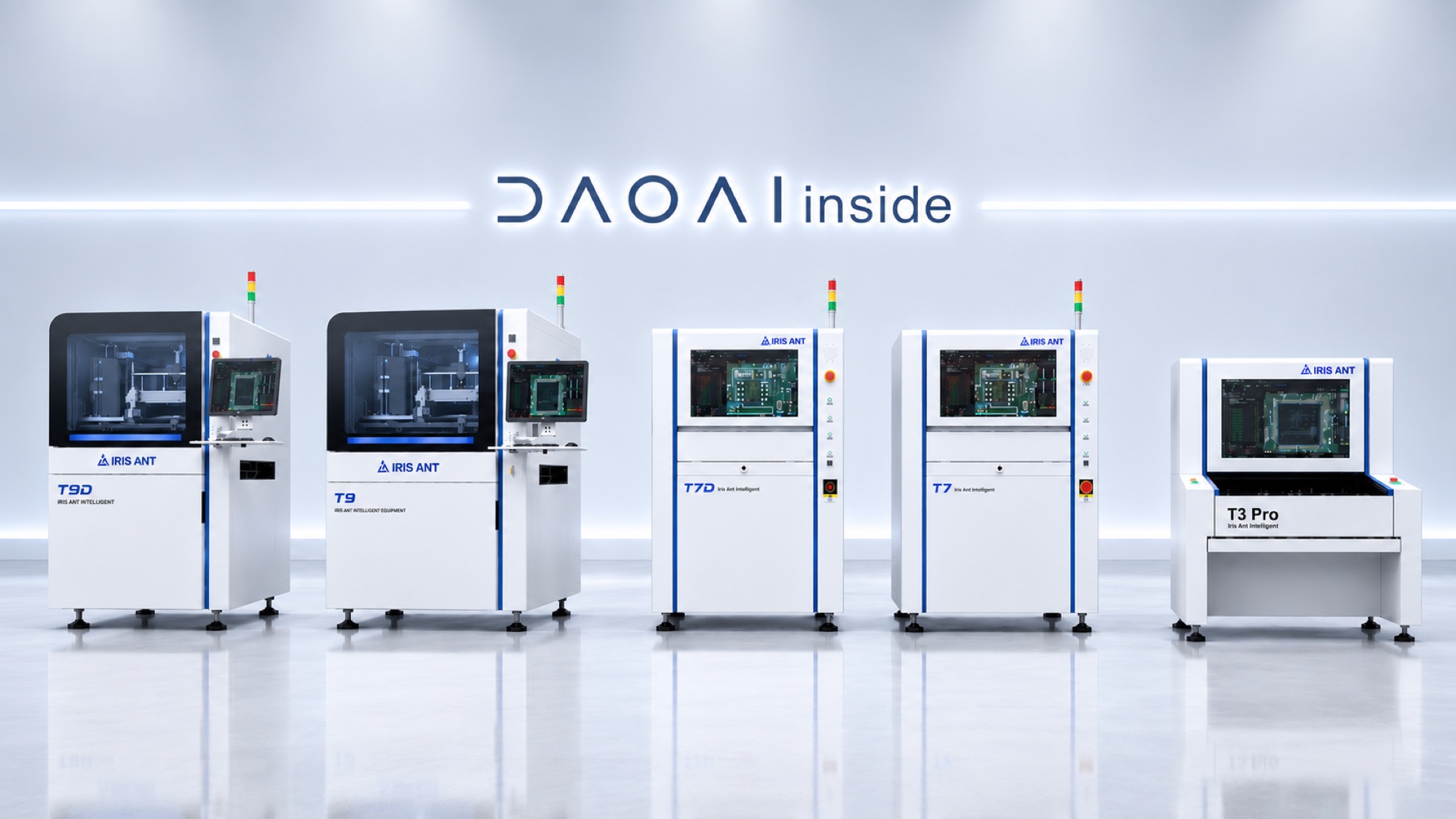
高速、高效率
專為現代SMT產線設計

1毫秒/元件
毫秒級檢測
即時檢測高密度板上的缺失元件、錯誤元件和極性問題,無運算瓶頸。

45 平方公分/秒
吞吐量
完美匹配高混合量 SMT 產線節拍,消除回流焊後檢測瓶頸。

CPU/GPU
平行處理架構
GPU 專注於處理複雜缺陷與 OCR,CPU 同步處理邏輯運算。真正的平行處理確保任務不互相等待,最大化硬體效率。
PCBA 檢測設備
全線搭載DaoAI AI AOI for PCBA AI檢測軟體
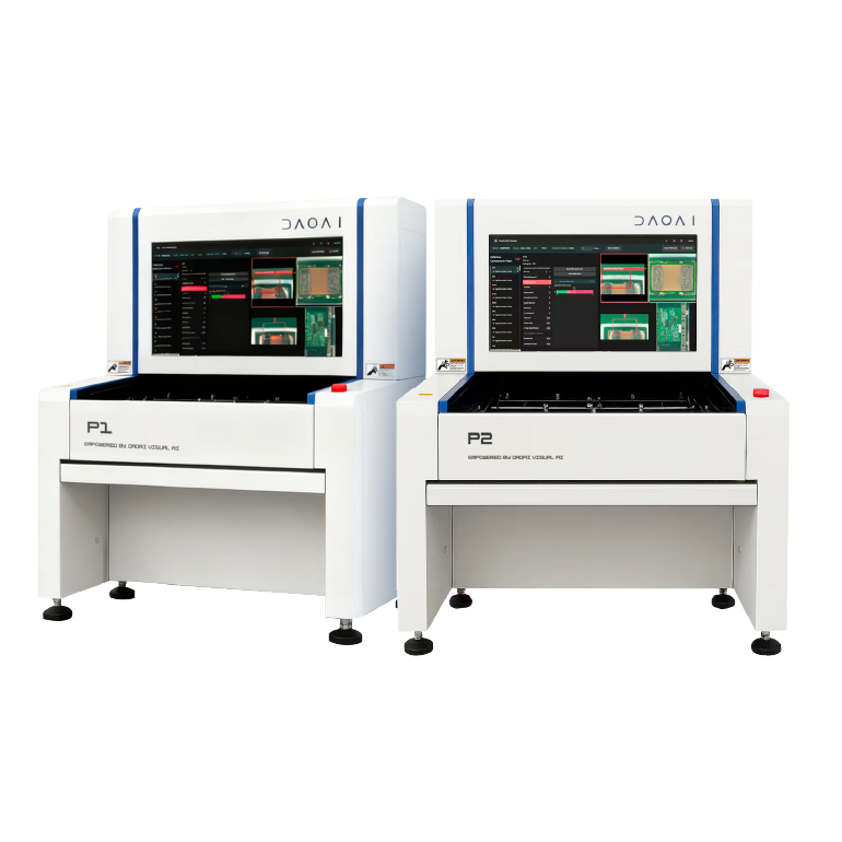
DaoAI P1/P2
離線式 · 手動上料適用場景高混合產量場景
相機/解析度P1: 5MP(15 微米)
P2: 12MP(10 微米)
P2: 12MP(10 微米)
成像系統10MP 遠心光學鏡頭
光源多光譜 RGB 六通道
最大 PCB 尺寸470 × 330 毫米
傳送帶手動上下板
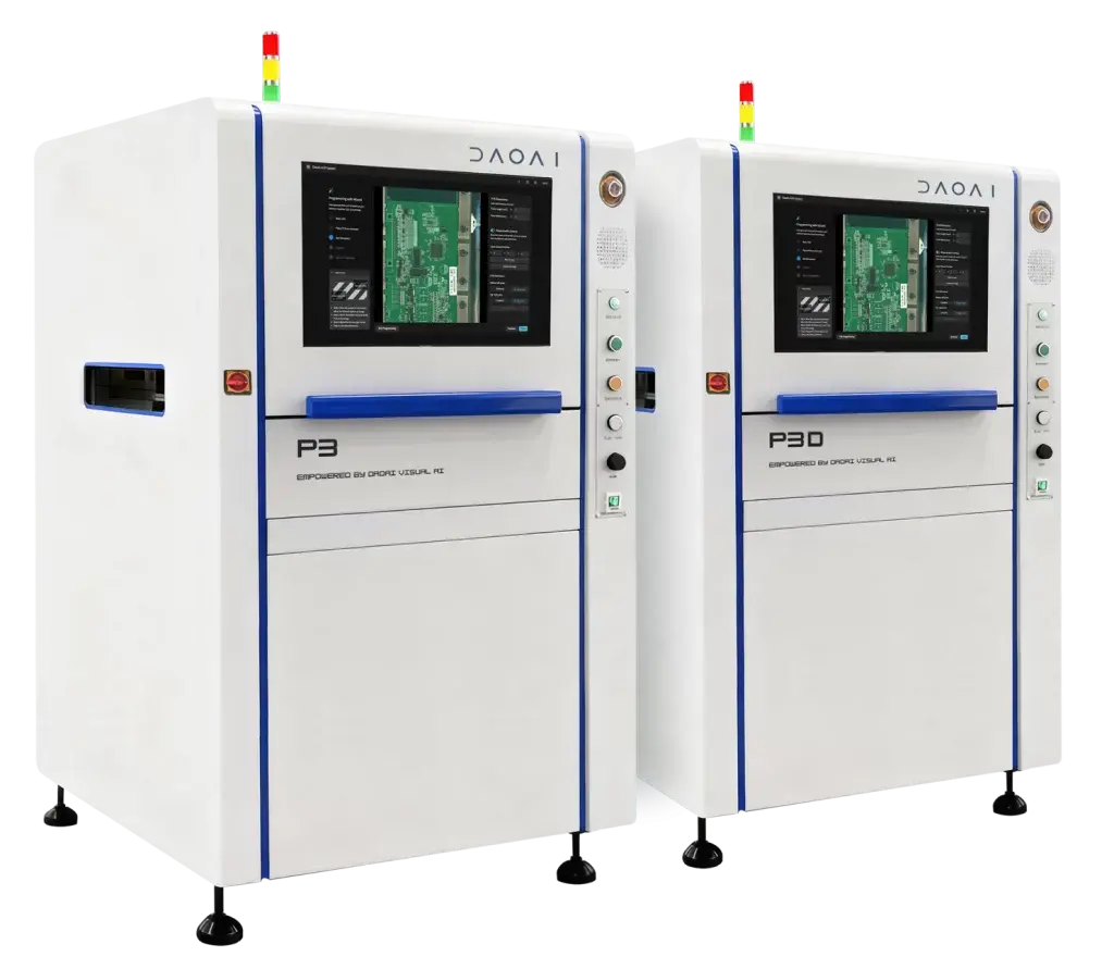
DaoAI P3/P3D
在線式 · 單軌/雙軌適用場景高產量 SMT 產線
相機26MP 高速全域快門相機
解析度10 微米/像素(FOV 38 × 30 毫米)
鏡頭10MP 遠心光學鏡頭
光源高亮度 RGB 同軸環形多角度 LED
PCB 尺寸50 × 50 – 500 × 825 毫米
PCB 厚度0.3 – 6 毫米
傳送帶單軌(P3)/ 雙軌(P3D)
計算您的 ROI
了解 AI 驅動 AOI 方案能為您節省多少成本
削減人工成本
每條產線每年節省約 20 萬至 30 萬新台幣。
賦能操作員
將設定工作從「僅限編程工程師」轉變為「操作員 30 分鐘上手」。
最大化設備利用率
將機器閒置時間重新轉化為有效生產時間。
年度節省
20萬
新台幣 – 30萬
新台幣
新台幣 – 30萬
新台幣
每條產線,每一年。
您的工廠數據
您的年度潛在節省金額
基於您的數據:
每條產線每週 NPI 次數:
每次 NPI 所需工時:
工程師時薪:
SMT 產線數量:
根據您的數據,您目前每年在各條 SMT 產線上的 AOI 編程支出為:
採用 DaoAI 的 AI 解決方案後,您可節省 40% 至 60% 的 AOI 編程時間。這表示:
Conservative
Estimate
(40% time
savings)
to
Optimistic
Estimate
(60% time
savings)
預計年度節省(中值):
聯絡我們獲取詳細 ROI 報告 →
離線式 2D AI AOI :DaoAI P1 與 P2 採用先進視覺 AI,實現 PCBA 檢測編程自動化。系統直接從樣板學習,可自動辨識元件、生成邊界框並定義缺陷閾值,將建程時間從數小時縮短至 5 分鐘。
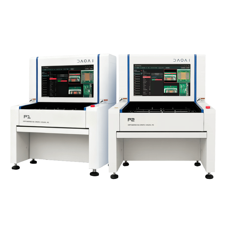
DaoAI P1/P2 規格說明
為速度、精度與適應性而設計
DaoAI P1
5MP 相機
解析度:15 微米
DaoAI P2
12MP 相機
解析度:10 微米
DaoAI P1
DaoAI P2
光學系統
相機
5 MP
12MP
Resolution
10 微米
15 微米
光源
Multispectral
ultra-high-speed RGB six-channel
lighting
Multispectral
ultra-high-speed RGB six-channel
lighting
Lens
Dual telecentric
optical lenses
Dual telecentric
optical lenses
輸送系統與 PCB 尺寸
PCB Size
0.5×50mm -
470×330mm
0.5×50mm -
470×330mm
PCB Thickness
0.5mm - 5mm
0.5mm - 5mm
Maximum PCB Warpage
Top25mm;Bottom110mm
Top25mm;Bottom110mm
Positioning Accuracy
±3mm
±3mm
Maximum Component Height
2.5mm
2.5mm
檢測能力
PCB Size
Missing
components, Reversed components,
Position offset, Polarity errors, Wrong
components, Component damage, Bent
leads, Foreign materials on PCB,
Contaminated or solder-stained gold
fingers, Glue overflow
Missing
components, Reversed components,
Position offset, Polarity errors, Wrong
components, Component damage, Bent
leads, Foreign materials on PCB,
Contaminated or solder-stained gold
fingers, Glue overflow
Solder Joint Inspection
Excess solder /
insufficient solder, Tombstoning, Solder
bridging, Cold solder / poor wetting,
Lifted leads, Solder balls, Post–wave
soldering defects (including
through-hole components)
Excess solder /
insufficient solder, Tombstoning, Solder
bridging, Cold solder / poor wetting,
Lifted leads, Solder balls, Post–wave
soldering defects (including
through-hole components)
Process Coverage
Supports
inspection of solder paste, red-glue
(SMT adhesive), and post–wave soldering
PCB assembly quality
Supports
inspection of solder paste, red-glue
(SMT adhesive), and post–wave soldering
PCB assembly quality
附加功能
Marking Function
PCB Fiducial
Mark, Panel Mark, Break-off Tab Mark
Recognition
PCB Fiducial
Mark, Panel Mark, Break-off Tab Mark
Recognition
Programming Function
CAD Data Import:
Automated region generation and
inspection parameter setupAutomatic
Component Library Indexing
CAD Data Import:
Automated region generation and
inspection parameter setupAutomatic
Component Library Indexing
Logging Function
Statistical
Process Control (SPC) and Data Reporting
Statistical
Process Control (SPC) and Data Reporting
Accessibility
Voice-Controlled
Operation
Voice-Controlled
Operation
檢測與自動配置能力
| 元件本體 | 極性 | IC 引腳 | 字元 | |
|---|---|---|---|---|
| 電容 |
|
|
|
|
| 電阻 |
|
|
|
|
| 多層片式電感 |
|
|
||
| 鋁電解電容 |
|
|
|
|
| 鉭電容 |
|
|
|
|
| 電阻陣列 |
|
|
|
|
| 功率電感 |
|
|
||
| LED |
|
|
|
|
|
SOT/SOD |
|
|
|
|
|
SOIC/SOP/TSOP/TSSOP/MSOP |
|
|
|
|
|
QFP |
|
|
|
|
|
QFN |
|
|
||
| TO-263/TO-252 |
|
|